Selectively Strained Two-Dimensional Heterostructures on the Cover
van der Waals (vdW) heterostructures (HSs) are super-crystals formed by stacking different two-dimensional (2D) materials. The weak vdW bonding between the crystals has prompted a goldmine of degrees of freedom, comprising chemical composition, thickness, order and relative twist angle of the HS single constituents. Semiconducting vdW HSs formed by transition metal dichalcogenides (TMDs) are especially investigated thanks to their excellent optical properties and the surprising physical effects they give rise to [1].
However, the achievement of high-performance optoelectronic devices remains a challenge due to the necessity to find HSs with efficient charge transfer between the different layers dictated by momentum-space matching between conduction band minima (CBM) and valence band maxima (VBM). Fine-tuning mechanisms to design ideal HSs are still lacking. To this regard, strain is a practical approach to tune the electronic properties of 2D crystals due to their inherent flexibility [2].
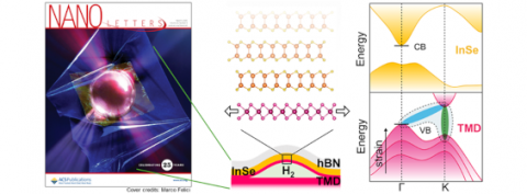
The front cover of the March issue of Nano Letters [3] features a novel paradigm conceived by Elena Blundo (previously in the OPERA group coordinated by Antonio Polimeni) and colleagues, whereby selective straining is applied to only one of the constituent materials of vdW HSs. The featured HSs are formed by MS2 (M = Mo or W) TMD monolayers and indium selenide (InSe; a vdW crystal) thin flakes. The strain applied to the former triggers a giant enhancement in the light emission efficiency of the latter.
The choice of InSe is grounded in its excellent properties, such as a high electron mobility and a quasi-direct and thickness-tunable optical bandgap [4], which make InSe particularly appealing for fast photodetectors operating from the ultraviolet to the near-infrared range. Though, the use of InSe for optoelectronic devices is hampered by its relatively low radiative efficiency stemming from the peculiar InSe CBM and VBM momentum-space configuration.
Elena Blundo, Federico Tuzi (PhD student in the OPERA group) and collaborators fabricated selectively strained HSs by deterministic deposition of thin InSe layers on highly strained, artificially created TMD monolayer micro-domes filled with hydrogen.
The selective strain application to TMD monolayers reshuffles their valence band structure and favours a mixing between defect states and the conduction band states. First-principle calculations and excitation resonant photoluminescence measurements unveil the formation of a type-I HS featuring an unprecedentedly efficient charge transfer from the TMD monolayers to the poorly emitting InSe. In turn, a one-to-three orders of magnitude enhancement of the emission efficiency of InSe is found thus largely improving the prospects of InSe in a wide range of optoelectronic applications.
The work was in a collaboration with the University of Nottingham (UK) and the NIMS Institute in Japan for the material growth, the IFN-CNR Institute for HS morphological studies and the University of Tor Vergata for the theory.
[1] L. Du L. et al., Moiré photonics and optoelectronics. Science 379, eadg0014 (2023)
[2] E. Blundo et al., Strain-tuning of the electronic, optical, and vibrational properties of two-dimensional crystals, Appl. Phys. Rev. 8, 021318 (2021)
[3] E. Blundo, F. Tuzi et al., Giant Light Emission Enhancement in Strain-Engineered InSe/MS2 (M = Mo or W) van der Waals Heterostructures, Nano Lett. 25, 3375 (2025); https://pubs.acs.org/toc/nalefd/25/9
[4] D. A. Bandurin et al., High electron mobility, quantum hall effect and anomalous optical response in atomically thin InSe, Nat. Nanotechnol. 12, 223 (2017)
Authors: Elena Blundo, Federico Tuzi, Marzia Cuccu, Michele Re Fiorentin, Giorgio Pettinari, Atanu Patra, Salvatore Cianci, Zakhar R. Kudrynskyi, Marco Felici, Takashi Taniguchi, Kenji Watanabe, Amalia Patanè, Maurizia Palummo, and Antonio Polimeni
Article: https://pubs.acs.org/toc/nalefd/25/9